Wanlin Group AndroidSBC · A133 payment terminal board custom design Flagship for India Buyers - Wholesale OEM and ODM Custom P
A133 payment terminal board custom design Flagship for India Buyers - Wholesale OEM and ODM Custom P
payment terminal board custom design - OEM and ODM Custom Payment Terminal Boards - India export OEM ODM wholesale
Product Scope and Support
Review the product configuration, interfaces, platform options, customization services and engineering support for this solution.
Information Needed for Selection
Share the use case, required interfaces, operating system, display requirements, quantity and target delivery schedule.
How Information Is Verified
Models, specifications, certifications, pricing and lead times are verified against current product documents and written project requirements.
Product Center
A133 payment terminal board custom design Flagship for India Buyers - Wholesale OEM and ODM Custom P
Availability: In stock
- Release Date:2026-09-30
- Product Description:payment terminal board custom design - OEM and ODM Custom Payment Terminal Boards - India export OEM ODM wholesale
- Consult Now
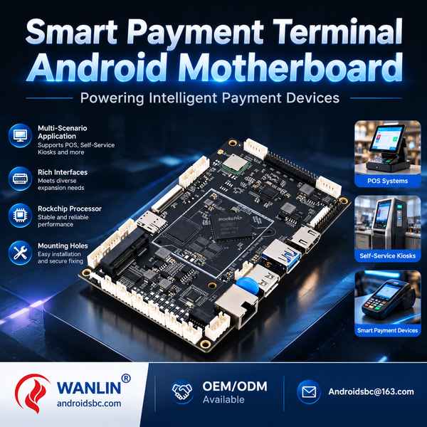
From September 30, 2026, India importers, payment terminal brands and retail integrators can source the A133-OD180 straight from Wanlin Group (Shenzhen, China), Allwinner A133 quad-core SoC, 4GB LPDDR4 + 32GB eMMC, 10.1-inch LVDS touch with HDMI secondary, Android 12.0 AOSP build for payment-only devices, 10/100M Ethernet with dual-band WiFi and Bluetooth 4.2 for fixed-lane counters, under the 2026 OEM and ODM Custom Payment Terminal Boards program: 4GB LPDDR4 + 32GB eMMC, with private-label and custom payment terminal programmes where the carrier board, memory and storage combination, radio set, printer and scan interfaces and firmware are built around the buyer's own product, built for the way India merchants and counter teams actually work. Wanlin Group as the smart payment terminal board supplier, exporter and original manufacturer now serves local partners, regional exclusive distributors and strategic OEM clients in more than 60 destination markets, and this export program is open to India buyers ordering at factory-direct terms.
Core parameters: Allwinner A133 quad-core SoC, 4x Cortex-A53 with PowerVR GE8300 graphics. CPU 4x ARM Cortex-A53 up to 1.6GHz, 64-bit architecture. GPU PowerVR GE8300 GPU, OpenGL ES 3.2. Render and security path PowerVR GE8300 render path sized for payment UI, amount display, QR presentation and signature capture. Video decode Hardware decode up to 4K@30fps H.265 and H.264 with 1080P@60fps across the mainstream codec range. Camera input Camera input for barcode imagers, document capture and face payment camera modules. Memory and storage 4GB LPDDR4 + 32GB eMMC. Operating system Android 12.0 AOSP build for payment-only devices, with OTA upgrade and signed firmware. Display and touch 10.1-inch 1280x800 LVDS panel with capacitive multi-touch and a secondary HDMI channel. Audio and signalling Speaker output with microphone input, voice prompt playback and a scan beep channel. Interfaces and I/O 1x LVDS or MIPI DSI display with capacitive touch, 1x HDMI secondary display, 1x camera input, 3x USB Host with 1x USB OTG, 1x RS232 with TTL UART option, 1x thermal printer head and cutter control, 1x scan engine UART, GPIO, I2C, SPI, PWM and ADC expansion. Networking 10/100M Ethernet with dual-band WiFi and Bluetooth 4.2 for fixed-lane counters. Power input 12 V DC input with an onboard buck stage, a separate supply path for the thermal printer head, RTC retention and scheduled power on/off for unattended duty. Duty profile Continuous counter duty with hardware watchdog, RTC retention, scheduled power on/off and auto power on after a mains cut; a wide-temperature build is available for unattended outdoor enclosures. PCB Smart payment terminal PCBA with onboard LPDDR and eMMC, display and touch interface, camera input, printer and scan-engine headers, SIM and TF card slots, Ethernet and a USB service path. Certifications CE / FCC / RoHS / REACH with EMV-relevant documentation support. Wanlin's 2026 export roadmap for India also covers custom memory and storage combos, printer and scan engine interface selection, contactless antenna placement, custom peripheral drivers, private-label branding and per-destination certification documentation packages.
Executive Summary - OEM and ODM Custom Payment Terminal Boards Export for Global B2B Buyers
Executive summary - 10 buyer-relevant points:
- Featured model A133-OD180, OEM and ODM Custom Payment Terminal Boards, Allwinner A133 quad-core SoC, 4x Cortex-A53 with PowerVR GE8300 graphics
- CPU 4x ARM Cortex-A53 up to 1.6GHz, 64-bit architecture
- GPU PowerVR GE8300 GPU, OpenGL ES 3.2
- Render and security path PowerVR GE8300 render path sized for payment UI, amount display, QR presentation and signature capture
- Video decode Hardware decode up to 4K@30fps H.265 and H.264 with 1080P@60fps across the mainstream codec range
- Memory and storage 4GB LPDDR4 + 32GB eMMC
- OS Android 12.0 AOSP build for payment-only devices, with OTA upgrade and signed firmware
- Display and touch 10.1-inch 1280x800 LVDS panel with capacitive multi-touch and a secondary HDMI channel
- MOQ 100 pcs, lead time 25-40 days, FOB Shenzhen / CIF / EXW / DDP supported, 36 months warranty
- Field reference: dual-source programme for a national rollout - supply interruption risk removed from the rollout plan
- Target buyer: payment device brand owners, private-label programme managers, overseas distributors building their own line, ODM houses and cross-border traders sourcing a factory partner
- Contact: Email: Androidsbc@163.com | Phone: +8613261677119 | Website: https://www.androidsbc.com
What follows is the fact set Wanlin shares with OEM and ODM Custom Payment Terminal Boards buyers before quotation: scope, commercial terms, compliance route and field record. Wanlin Group operates its own 12,000 m2 manufacturing facility in Shenzhen with 8 SMT lines, 4 AOI inspection stations and 2,400 m2 of cleanroom assembly, exporting smart payment terminal boards to 60+ countries under the AndroidSBC brand. Total cost of ownership for an AndroidSBC OEM and ODM Custom Payment Terminal Boards deployment typically runs 42-60% below x86-based cashier hardware once per-device OS licensing and patch handling are counted. For India, this article maps the model line, the economics and the compliance route specific to your market.
Global OEM and ODM Custom Payment Terminal Boards Market Overview and 2026 Buyer Demand
Long-life programmes are now written into transport and public-sector tenders. A locked BSP, a component last-time-buy window and a price lock are worth more than a lower unit price to any operator who has recertified a device twice.
Regional compliance for India is anchored on BIS registration, WPC ETA radio approval and BEE-relevant documentation. Cross-border buyers are advised to verify the certification scope, the contactless behaviour and the software build of every board before import, since some China-supplied boards ship without destination radio approval, without the payment documentation the acquirer asks for, or without the Android build the project actually needs, and any of those gaps can stall customs clearance or a scheme review.
Reference: Wanlin Group 2026 smart payment terminal export program documentation, Rockchip and Allwinner platform datasheets, field deployment records 2024-2026.
OEM and ODM Custom Payment Terminal Boards Engineering Architecture and Hardware Platform
The smart payment terminal family is engineered on three pillars: (1) an Allwinner A133 quad-core SoC, 4x Cortex-A53 with PowerVR GE8300 graphics compute block with PowerVR GE8300 render path sized for payment UI, amount display, QR presentation and signature capture; (2) a display and capture pipeline built around Hardware decode up to 4K@30fps H.265 and H.264 with 1080P@60fps across the mainstream codec range; (3) a software layer pairing Android 12.0 AOSP build for payment-only devices, with OTA upgrade and signed firmware with OTA tooling, device management and the Allwinner A133 Android BSP, AOSP build support, peripheral driver kit and the AndroidSBC SDK kit. This architecture delivers continuous counter and unattended duty at a cost point that undercuts cashier PCs while keeping the payment, print and scan response operators expect.
Three sub-modules define the engineering depth:
- Compute module - Allwinner A133 quad-core SoC, 4x Cortex-A53 with PowerVR GE8300 graphics. 4x ARM Cortex-A53 up to 1.6GHz, 64-bit architecture handles the tender flow, catalogue screens, signature capture and on-device vision work inside a fanless terminal shell.
- Display and capture module - 10.1-inch 1280x800 LVDS panel with capacitive multi-touch and a secondary HDMI channel. Camera input for barcode imagers, document capture and face payment camera modules covers the camera input used for face payment, document capture and proof of purchase, so one device closes the transaction and records the evidence.
- Peripheral and management module - 1x LVDS or MIPI DSI display with capacitive touch, 1x HDMI secondary display, 1x camera input, 3x USB Host with 1x USB OTG, 1x RS232 with TTL UART option, 1x thermal printer head and cutter control, 1x scan engine UART, GPIO, I2C, SPI, PWM and ADC expansion. Headless recovery is supported through the USB service path, and the toolchain covers Allwinner A133 Android BSP, AOSP build support, peripheral driver kit and the AndroidSBC SDK kit, OTA upgrade, boot animation customization, pre-installed app support and launcher customization for remote fleet management.
Mechanically the board is a Smart payment terminal PCBA with onboard LPDDR and eMMC, display and touch interface, camera input, printer and scan-engine headers, SIM and TF card slots, Ethernet and a USB service path, which is why it drops into countertop shells, kiosk housings and wall-mounted enclosures without a tooling change.
Featured Model - A133-OD180 Flagship Technical Signature
The featured model is A133-OD180, part of the OEM and ODM Custom Payment Terminal Boards family, configured in this batch with 4GB LPDDR4 memory and 32GB eMMC storage. FOB Shenzhen reference price is $93.50 per piece at MOQ 100 pcs, with bulk tier pricing from $80.41 to $104.72 depending on memory and storage combination, radio set, regional certification and packaging artwork. Lead time is 25-40 days from PO confirmation and 30% T/T deposit receipt, with a 36-month warranty.
The technical signature of A133-OD180 on this configuration is documented below. Every parameter is verified by our Shenzhen lab against the printer duty profile, the contactless read behaviour of the final enclosure and the electrical limits of IEC / UL 62368-1.
| Specification | Value |
|---|---|
| soc_platform | Allwinner A133 quad-core SoC, 4x Cortex-A53 with PowerVR GE8300 graphics |
| cpu_core | 4x ARM Cortex-A53 up to 1.6GHz, 64-bit architecture |
| gpu_3d | PowerVR GE8300 GPU, OpenGL ES 3.2 |
| render_security_path | PowerVR GE8300 render path sized for payment UI, amount display, QR presentation and signature capture |
| video_decode | Hardware decode up to 4K@30fps H.265 and H.264 with 1080P@60fps across the mainstream codec range |
| camera_input | Camera input for barcode imagers, document capture and face payment camera modules |
| memory_storage | 4GB LPDDR4 + 32GB eMMC |
| os_android | Android 12.0 AOSP build for payment-only devices, with OTA upgrade and signed firmware |
| display_touch | 10.1-inch 1280x800 LVDS panel with capacitive multi-touch and a secondary HDMI channel |
| audio_signalling | Speaker output with microphone input, voice prompt playback and a scan beep channel |
| interfaces_io | 1x LVDS or MIPI DSI display with capacitive touch, 1x HDMI secondary display, 1x camera input, 3x USB Host with 1x USB OTG, 1x RS232 with TTL UART option, 1x thermal printer head and cutter control, 1x scan engine UART, GPIO, I2C, SPI, PWM and ADC expansion |
| networking | 10/100M Ethernet with dual-band WiFi and Bluetooth 4.2 for fixed-lane counters |
| power_input | 12 V DC input with an onboard buck stage, a separate supply path for the thermal printer head, RTC retention and scheduled power on/off for unattended duty |
| duty_profile | Continuous counter duty with hardware watchdog, RTC retention, scheduled power on/off and auto power on after a mains cut; a wide-temperature build is available for unattended outdoor enclosures |
| pcb_mechanics | Smart payment terminal PCBA with onboard LPDDR and eMMC, display and touch interface, camera input, printer and scan-engine headers, SIM and TF card slots, Ethernet and a USB service path |
| certifications | CE / FCC / RoHS / REACH with EMV-relevant documentation support |
| use_case | private-label and custom payment terminal programmes where the carrier board, memory and storage combination, radio set, printer and scan interfaces and firmware are built around the buyer's own product |
OEM and ODM Custom Payment Terminal Boards Application Scenarios across Deployment Sites
Deployment notes below come from live OEM and ODM Custom Payment Terminal Boards installations on several continents, each carrying a site, a unit count and a measured outcome.
Scenario 1: dual-source programme for a national rollout (Chennai, India). A national programme required two board sources on the same mechanical footprint, and the second source was qualified on the same carrier drawing with the same driver set and the same BSP baseline. Measured result: supply interruption risk removed from the rollout plan and qualification completed in 9 weeks.
Scenario 2: private-label countertop line for a distributor (Eindhoven, Netherlands). A European distributor launched its own countertop terminal line on a redesigned carrier that keeps the board footprint but moves the printer header and the Ethernet jack to the back panel of its own enclosure. Measured result: time from design freeze to first shipment was 11 weeks and enclosure tooling cost avoided entirely.
Scenario 3: small-batch custom run for a niche format (Sarajevo, Bosnia). A niche operator ordered 600 units of a narrow-format terminal with a rotated display and a side-mounted printer, and the factory ran it on the same SMT line as its standard boards. Measured result: unit cost held within 8% of the standard board and minimum order accepted at 600 rather than 5,000.
Scenario 4: certification package build for a regulated launch (Doha, Qatar). A regulated launch required a per-model documentation pack, and the factory supplied DoC templates, test report copies, label artwork and a pre-validated compliance set before shipment. Measured result: importer certification lead time fell from 11 weeks to 2 and launch date held without a slip.
Scenario 5: white-label terminal for a regional acquirer (Monterrey, Mexico). An acquirer launched a white-label terminal with its own silk-screen, boot animation, launcher and packaging, with per-unit provisioning so each device ships bound to its merchant ID. Measured result: merchant onboarding time fell from 5 days to 45 minutes and first-year device returns fell 64%.
AndroidSBC OEM and ODM Custom Payment Terminal Boards Competitive Advantages for Cross-Border Buyers
The smart payment terminal board and the wider AndroidSBC payment device portfolio deliver eight advantages for cross-border B2B buyers sourcing from Chinese manufacturers:
- Source-factory pricing - Wanlin operates the SMT lines, so FOB Shenzhen pricing runs 42-60% below western-branded payment terminals with no per-device licence fee.
- Tender coverage - QR, barcode, NFC contactless, EMV chip and magnetic stripe on one board, with secure boot, tamper inputs and key storage where the scheme asks for it.
- Printer and scan integration - thermal receipt printer head and cutter control plus a scan engine UART on the board, so receipt and scan do not need a second controller.
- Display coverage - a merchant channel and a customer channel on one board across LVDS, eDP, MIPI DSI and HDMI, which removes the pole display and its power supply from the kit.
- Offline behaviour - transaction and scan queueing that posts when the signal returns, because the counters and kiosks that matter most are the ones where coverage fails.
- Peripheral and service path - 1x LVDS or MIPI DSI display with capacitive touch, 1x HDMI secondary display, 1x camera input, 3x USB Host with 1x USB OTG, 1x RS232 with TTL UART option, 1x thermal printer head and cutter control, 1x scan engine UART, GPIO, I2C, SPI, PWM and ADC expansion, covering printer, scanner, camera, RFID, SIM and TF, GPIO, RS232, RS485 and serial expansion, plus a USB service port for field recovery.
- Multi-OS flexibility - Android 12.0 AOSP build for payment-only devices, with OTA upgrade and signed firmware, so GMS devices, AOSP payment builds and private-label launcher programmes run on one board.
- Unattended reliability - hardware watchdog, RTC retention, scheduled power on and off, auto power on after a mains cut and OTA with a canary ring.
Combined, these advantages let AndroidSBC partners win retail, banking, transport and private-label programmes, secure regional distribution rights, and serve end customers under their own brand at a landed cost 35-45% below legacy suppliers.
OEM and ODM Custom Payment Terminal Boards Certifications, Electrical Performance and Assembly Notes
The A133-OD180 carries CE / FCC / RoHS / REACH as standard scope. Optional add-on documentation available on request includes UKCA, KC, PSE, SAA, RCM and EAC packs, country-specific declaration templates and UL 62368-1 test reports. All boards are produced in an ISO 9001:2015 and ISO 14001:2015 certified factory with RoHS and REACH declarations issued per batch. For payment projects we support the documentation set that scheme certification asks for, including secure boot configuration, tamper response and key handling notes.
Electrical performance is characterised against the final enclosure: 12 V DC input with an onboard buck stage, a separate supply path for the thermal printer head, RTC retention and scheduled power on/off for unattended duty, with the printer head supplied on its own power path and the contactless antenna tuned with the shell closed. The board is specified for Continuous counter duty with hardware watchdog, RTC retention, scheduled power on/off and auto power on after a mains cut; a wide-temperature build is available for unattended outdoor enclosures, which covers countertop shells, kiosk housings and wall-mounted enclosures with no fan and no vent.
Assembly and integration notes every integration team should run through before closing an enclosure:
- Budget the thermal printer head supply as a separate power path with its own bulk capacitance, because the head draws a sharp current pulse on each printed line and will brown out the logic rail if it shares it
- Route the LVDS or eDP flex away from the printer harness and the mains entry, and keep it inside the bend radius drawn for the connector, since display noise shows up as flicker only after the enclosure is closed
- Place the contactless antenna away from the printer mechanism, the shielding can and any metal bracket, then tune it with the final enclosure closed, because detuning appears as read failures at the counter rather than in the lab
- Configure secure boot, the tamper detection inputs and key storage before the security review, since payment schemes ask for the key handling description and the tamper response during certification rather than after
- Bond the shielding can to chassis ground at the points drawn on the carrier and keep the Ethernet transformer side of the board free of signal copper, since EMC failures at the test house usually trace back to a floating can
- Support the PCBA on all screw bosses and keep it flat in the housing, because a flexed board cracks BGA joints under transport vibration and the failure surfaces weeks later in the field
- Give the USB service port ESD protection on the data lines and keep it reachable without opening the payment compartment, because tamper-evident seals mean a sealed unit can no longer be recovered on site
Cross-border buyers should note that payment terminal compliance combines product marking, radio certification, safety evaluation and the scheme documentation the acquirer asks for. For India specifically, importers should confirm BIS registration, WPC ETA radio approval and BEE-relevant documentation before shipment. Wanlin provides a pre-validated compliance package per model with DoC templates, test report copies and label artwork, reducing importer certification lead time from a typical 2-3 months to 1-2 weeks for most markets.
OEM and ODM Custom Payment Terminal Boards Economics, MOQ, Lead Time and Logistics Math
For a first-time buyer ordering 1,000 pieces of the A133-OD180, the economics stack is:
| Cost Layer | USD per piece | USD for 1000 pcs |
|---|---|---|
| FOB Shenzhen factory price | $93.50 | $93500.00 |
| + Sea freight FCL 40HQ (estimated) | $2.10 | $2100.00 |
| CIF destination port | $95.60 | $95600.00 |
| + Customs duty 3%-10% (region dependent) | $0.64 | $637.10 |
| + Local delivery + warehousing | $3.80 | $3800.00 |
| DDP landed cost | $100.04 | $100040.00 |
Sample order cost is USD 60 per SKU refundable against the first bulk order above MOQ. 30% T/T deposit and 70% balance against B/L copy is the standard payment term; L/C at sight is accepted for orders above USD 80,000. Production lead time is 25-40 days, warranty is 36 months, and free DOA replacement applies within 60 days of receipt.
OEM and ODM Custom Payment Terminal Boards FAQ - OEM, ODM, MOQ, Lead Time, Partnership
Below are eight frequently asked questions from cross-border buyers sourcing smart payment terminal boards from China. Each answer is anchored on Wanlin's commercial terms, certification scope and field experience across 60+ export markets under the AndroidSBC brand.
What is the difference between OEM and ODM for OEM and ODM Custom Payment Terminal Boards?
Answer: OEM (Original Equipment Manufacturer) means Wanlin Group builds the board, the payment terminal or the finished device under your brand with your PCB silk-screen, logo, packaging and SKU. ODM (Original Design Manufacturer) means we redesign the carrier board, memory and storage combination, radio set, printer and scan engine interfaces, firmware or enclosure around your project. Both run from the same Shenzhen factory and the same firmware team: OEM lead time is 25-40 days and ODM 25-40 days including pre-compliance checks. Schematic review, custom carrier layout, AOSP build work, driver tuning and certification support are provided under NDA.
Which smart payment terminal board should I source for my application?
Answer: Eight selection rules for cross-border buyers:
- (1) Desktop and countertop terminals: DT110 / DT130 class with dual-screen output, an on-board receipt printer path and a customer-facing confirmation screen.
- (2) Self-service and unattended kiosks: SK120 / SK140 with a scan engine, a printer, GPIO release control and a watchdog tuned for unattended duty.
- (3) Retail and supermarket lanes: RC120 / RC150 with a barcode scanner, a scale link over serial and a loyalty prompt on the customer screen.
- (4) Restaurant and hospitality: RH120 / RH140 with bill splitting, tip-on-customer-screen, voice prompt of the amount and a kitchen display link.
- (5) Face recognition and biometric payment: FB150 / FB170 with on-device matching, liveness handling, secure boot, tamper inputs and key storage.
- (6) Parking, transport and ticketing: TP130 / TP150 with ticket scanning, GPIO barrier release, RS485 device control and a wide-temperature build.
- (7) Banking, government and public service: BP130 / BP160 with a stamped official receipt path, an auditable transaction ID and wired connectivity.
- (8) Private-label programmes and redesign work: OD170 / OD180 with carrier redesign, BSP porting, signed firmware, per-unit provisioning and a last-time-buy window.
What software support comes with the boards?
Answer: Every board ships with the Android image (Android 12.0 AOSP build for payment-only devices, with OTA upgrade and signed firmware), BSP source access, driver documentation, SDK material and OTA tooling. The build supports GMS where the destination market and product category qualify; for payment-only projects that do not need Google services, the same hardware runs a full AOSP build, which also lowers unit cost. Kiosk-mode launchers, auto-start app configuration, custom boot animation, scheduled behaviour and remote device management agents are part of the standard integration work. The media stack covers the video, audio and image formats listed in the platform section, and the payment stack covers QR, barcode, NFC contactless, EMV chip and magnetic stripe paths with hardware backed key storage where the project requires it.
How do Wanlin smart payment terminal boards compare with branded terminals and x86 cashier boxes?
Answer: Because Wanlin builds the boards rather than reselling them, landed cost typically runs 42-60% below western-branded payment terminals and 25-38% below a resold retail device on equivalent radio, display and printer support. On the engineering side, this configuration brings Allwinner A133 quad-core SoC, 4x Cortex-A53 with PowerVR GE8300 graphics, 4x ARM Cortex-A53 up to 1.6GHz, 64-bit architecture and PowerVR GE8300 GPU, OpenGL ES 3.2, with the BSP covering Android 12.0 AOSP build for payment-only devices, with OTA upgrade and signed firmware. Licensing cost also disappears: cashier PCs carry per-device OS licence fees and patch cycles, while the Android build carries none. The compact terminal PCBA also drops into enclosures that were designed around a larger device, which usually removes a second controller and a second power supply from the kit.
Can the board drive the displays, the printer and the full peripheral set?
Answer: Yes. 10.1-inch 1280x800 LVDS panel with capacitive multi-touch and a secondary HDMI channel. The peripheral stack covers thermal receipt printers with cutter control, 1D and 2D scan engines over UART, NFC and contactless readers, magnetic stripe and IC card readers, fingerprint modules, face cameras over MIPI CSI, RFID readers, SIM and TF card slots, GPIO and I2C or SPI expansion, plus a USB service path for field recovery. Audio covers speaker output, voice prompt playback, microphone capture and an intercom headset path. Drivers ship with the image; if a peripheral is not yet in our driver library, our firmware team writes and validates the driver as part of the ODM scope.
What are the MOQ, lead time, trade terms, sample policy and warranty?
Answer: MOQ is 100 pcs per model. Lead time is 25-40 days for standard configurations and 25-40 days for ODM customization. Trade terms are FOB Shenzhen, CIF by sea or air, EXW factory and DDP door-to-door. Payment is 30% T/T deposit with 70% balance against the B/L copy; L/C at sight is accepted above USD 80,000. Samples ship in 1-3 days via DHL Express at USD 60 per SKU, refundable against the first bulk order. Warranty is 36 months, with free DOA replacement within 60 days of receipt.
Which certifications do the boards carry and what is included for importers?
Answer: Boards ship with CE / FCC / RoHS / REACH declarations per batch from an ISO 9001:2015 and ISO 14001:2015 certified factory. UKCA, KC, PSE, SAA, RCM, EAC and UL 62368-1 report documentation is available on request, and BIS registration, WPC ETA radio approval and BEE-relevant documentation. For payment projects we also support the documentation set that scheme certification asks for, including secure boot configuration, tamper response description and key handling notes. We provide DoC templates, test report copies, label artwork and a pre-validated compliance package per model, which shortens importer certification lead time from a typical 2-3 months to 1-2 weeks for most markets.
What customization and partnership options does Wanlin offer?
Answer: Customization scope:
- (1) Branding - custom PCB silk-screen, private-label logo on board and enclosure, custom SKU, packaging and boot animation.
- (2) Firmware - custom launcher, kiosk lock-down, pre-installed apps, multilingual UI packs, custom boot logo and a signed OTA channel.
- (3) Hardware - carrier board redesign, memory and storage combinations, radio set selection, printer and scan engine interface placement, contactless antenna routing, SIM and TF slot layout and display channel selection.
- (4) Software - AOSP build service, BSP porting, peripheral driver development, SDK modules, remote device management agent integration and API work against your own payment application.
- (5) Delivery - DDP shipping, overseas-warehouse labelling, per-batch serial and key provisioning.
Wanlin Global Partner Stories - Real Project References
Partner projects below span 2024-2026 across 60+ destination markets. Each row carries a city, the application and the outcome the buyer measured.
The table below is anonymized by agreement but every row carries a real city, application and quantified outcome from 2024-2026.
| City | Application | Outcome |
|---|---|---|
| Auckland, New Zealand | six-year long-life transport programme, 3,400 units | board revision changes across the programme fell to zero and three recertifications were avoided |
| Chennai, India | dual-source national programme, 12,000 units | supply interruption risk left the rollout plan and qualification finished in 9 weeks |
| Monterrey, Mexico | white-label terminal line for a regional acquirer, 4,200 units | merchant onboarding fell from 5 days to 45 minutes and first-year returns dropped 64% |
| Doha, Qatar | regulated launch documentation package, 1,600 units | importer certification lead time fell from 11 weeks to 2 and the launch date held |
Partnership Models - Authorized Reseller, Regional Distributor, Strategic OEM
Wanlin offers three partnership tiers for cross-border buyers of OEM and ODM Custom Payment Terminal Boards:
- Authorized Reseller - annual volume USD 20,000+, list price, no exclusivity, standard 36-month warranty, dedicated account manager with a response within 4 business hours.
- Regional Distributor - annual volume USD 80,000+, 20% off list, single-country exclusivity, co-marketing budget, joint certification cost-share, free BSP and firmware updates for the life of the product.
- Strategic OEM Partner - annual volume USD 250,000+, 30% off list, multi-country exclusivity, dedicated engineering team, joint roadmap, 18-month price lock and one joint trade-show booth per year at GITEX Global, Money20/20, Canton Fair or the Hong Kong Electronics Fair in Hong Kong, China on a cost-share basis.
All partners receive free certification documentation and test report copies, custom Android image support, free DOA replacement within 60 days, per-batch serial and key provisioning, and a sample programme with USD 60 per SKU refundable against the first bulk order above MOQ.
Conclusion - How to Start Your OEM and ODM Custom Payment Terminal Boards Sourcing Today
Wanlin Group's 2026 smart payment terminal export program is open to B2B buyers, regional distributors, cross-border traders and OEM/ODM partners in India and 60+ destination markets. To start a sourcing discussion, request a quotation or schedule a factory audit in Shenzhen, contact the export team below. Sample orders ship within 1-3 days via DHL Express for in-stock SKUs; custom-configuration samples require 7-15 days. Standard lead time for bulk OEM orders is 25-40 days, and Strategic OEM Partner applications are reviewed quarterly.
We invite India buyers, export traders and trading companies to build long-term cooperation with Wanlin Group as your China-based OEM/ODM partner, regional exclusive distributor or strategic global supplier under the AndroidSBC brand. Wanlin is the manufacturer behind the smart payment terminal board line, the SMT lines and aging rooms behind every batch, and this export program. Let's build the OEM and ODM Custom Payment Terminal Boards supply chain together.
Model: A133-OD180
Platform: Allwinner A133 quad-core SoC, 4x Cortex-A53 with PowerVR GE8300 graphics
CPU: 4x ARM Cortex-A53 up to 1.6GHz, 64-bit architecture
GPU: PowerVR GE8300 GPU, OpenGL ES 3.2
Render / security: PowerVR GE8300 render path sized for payment UI, amount display, QR presentation and signature capture
Video: Hardware decode up to 4K@30fps H.265 and H.264 with 1080P@60fps across the mainstream codec range
Camera input: Camera input for barcode imagers, document capture and face payment camera modules
Memory: 4GB LPDDR4
Storage: 32GB eMMC
OS: Android 12.0 AOSP build for payment-only devices, with OTA upgrade and signed firmware
Display and touch: 10.1-inch 1280x800 LVDS panel with capacitive multi-touch and a secondary HDMI channel
Audio: Speaker output with microphone input, voice prompt playback and a scan beep channel
Network: 10/100M Ethernet with dual-band WiFi and Bluetooth 4.2 for fixed-lane counters
Interfaces: 1x LVDS or MIPI DSI display with capacitive touch, 1x HDMI secondary display, 1x camera input, 3x USB Host with 1x USB OTG, 1x RS232 with TTL UART option, 1x thermal printer head and cutter control, 1x scan engine UART, GPIO, I2C, SPI, PWM and ADC expansion
Power: 12 V DC input with an onboard buck stage, a separate supply path for the thermal printer head, RTC retention and scheduled power on/off for unattended duty
Field duty: Continuous counter duty with hardware watchdog, RTC retention, scheduled power on/off and auto power on after a mains cut; a wide-temperature build is available for unattended outdoor enclosures
PCB: Smart payment terminal PCBA with onboard LPDDR and eMMC, display and touch interface, camera input, printer and scan-engine headers, SIM and TF card slots, Ethernet and a USB service path
Cert: CE / FCC / RoHS / REACH with EMV-relevant documentation support
MOQ / Lead / Warranty: 100 pcs / 25-40 days / 36 months
FOB Shenzhen reference price: $93.50 per piece at MOQ 100 pcs
Region: India
Contact: Email: Androidsbc@163.com | Phone: +8613261677119 | Website: https://www.androidsbc.com
- Wanlin Group, Building B, Building 1, Beisida Medical Device Building, 28 Nantong Avenue, Baolong Community, Baolong Sub-district, Longgang District, Shenzhen, Guangdong, China
- Manufacturer: Wanlin Group / Brand: AndroidSBC / Site: www.androidsbc.com
- Export service: Email: Androidsbc@163.com | Phone: +8613261677119 | Website: https://www.androidsbc.com
- Form factor: OEM and ODM Custom Payment Terminal Boards / Platform: Allwinner A133 quad-core SoC / PCB: Smart payment terminal PCBA with onboard LPDDR and eMMC, display and touch interface, camera input, printer and scan-engine headers, SIM and TF card slots, Ethernet and a USB service path
- Country compliance for India: BIS registration, WPC ETA radio approval and BEE-relevant documentation
Category
News and Trends
- Payment Terminal Printer Board Export, WF-SPT-12, AndroidSBC, Ottawa
- Interactive Payment Kiosk Board, WF-SPT-01, AndroidSBC, Ottawa
- Rear Camera Payment Terminal Board, WF-SPT-02, AndroidSBC, Ottawa
- Laser Scanner Payment Terminal Board with OTA Updates, WF-SPT-03, AndroidSBC, Ottawa
- Contactless Payment Terminal Board with OTA Updates, WF-SPT-04, AndroidSBC, Ottawa
- 5.5-Inch Touch Payment Terminal Board for Retail Checkout, WF-SPT-01, AndroidSBC, Ottawa
- 1GB LPDDR4 Payment Terminal Board for Retail Checkout, WF-SPT-06, AndroidSBC, Ottawa
- Cortex-A76 Payment Terminal Motherboard, WF-SPT-04, AndroidSBC, Ottawa
- Handheld POS Scanner Board Export, WF-POSH-08, AndroidSBC, Ottawa
- Hotel Handheld POS Board, WF-POSH-01, AndroidSBC, Ottawa